With the improvement of people's living standards and the growing demand for security and defense in work and living environment, video surveillance systems have developed rapidly in recent years. Traditional PC-based video surveillance systems have some disadvantages such as inconvenient installation and inability to use in harsh environments. This is a new video surveillance system. With the rapid development of ultra-large-scale integrated circuits and embedded software and hardware technologies in recent years, especially the emergence of embedded chips such as DSP and PowerPC, the application of embedded processors to video surveillance systems not only overcomes the above-mentioned PC-based systems. Some of the shortcomings, along with its powerful features, rich peripheral interfaces and high programmability, make video surveillance hardware and software easier to implement. It is precisely because of the increasingly high cost performance plus the small size, low cost and other unique advantages, so that embedded chips have gradually gained a place in the field of video surveillance.
1 System Overview
The universal video surveillance system designed in this paper adopts the special multimedia chip TMS320DM642 (referred to as "DM642") produced by TI in 2002 as the processor, which can realize simultaneous acquisition of 4 channels of audio and video, and supports complex audio and video compression algorithms (such as MPEG4 standard). ), the collection, playback and storage of audio and video can be carried out 24 hours a day.
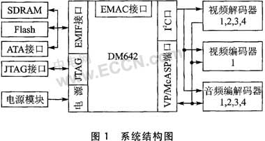
The working process of the system is as follows: After the system is powered on or reset, the program is loaded from the Flash, the initialization of the chip and the configuration of the peripheral hardware are completed, and then the image acquisition is started. The DM642 controls other chips in the system through the I2C port. The analog video signal collected from the camera is converted into a digital video signal by the video decoder and sent to the video channel (VP port) of the DM642; the synchronously collected analog audio signal passes through After the audio codec is analog-to-digital converted, it is sent to the audio channel of the DM642 (McASP port). The DM642 compresses the received digital video signal and digital audio signal with the MPEG4 standard code, and then stores the data in the file format to the local hard disk through the ATA interface extended by the DM642 for later recall. The system is mainly composed of the following modules: DM642 module, storage module, video and audio module, power module, etc. The system structure is shown in Figure 1.
 |
2 DM642 module
The DM642 is based on the C64x core and adds a lot of peripherals and interfaces to it. Therefore, it is more widely used and practical in practical engineering. The system uses a 50 MHz crystal as the DSP's external clock input, which is multiplied by an internal phase-locked loop and produces a 600 MHz operating frequency. The DM642 uses a level 2 cache structure (L1 and L2) to greatly improve the running performance of the program. The on-chip 64-bit EMIF (External Memory Interface) interface can be seamlessly connected to SDRAM, Flash and other storage devices, greatly facilitating the movement of a large amount of data. More importantly, as a dedicated video processing chip, the DM642 includes three dedicated video ports (VP0 to VP2) for receiving and processing video and audio data, improving the performance of the entire system. In addition, the DM642's own EMAC port and the ATA port extended from the EMIF port provide a storage channel for the massive data generated after processing.
3 video and audio modules
In the design, the VP0 of the DM642, the A channel of the VP1, and the A and B channels of the VP2 are all configured in a video acquisition mode, and four video signals can be simultaneously acquired. If local playback is required, set the A channel of the VP0 port to the playback mode. At this time, up to 3 video signals can be acquired. In addition, the B channels of VP0 and VP1 are configured as McASP functions for audio processing. The data between the DM642 and the video and audio codec chips are transmitted through these dedicated ports, but the control of these chips is realized through the I2C bus.
3.1 Video input section
To use the analog camera for video data acquisition, the video decoding chip is used to digitize the collected analog data, and then sent to the video port of the DM642 for processing. Here, four TVP5150A produced by TI Company are selected, and the connection with DM642 is shown in Figure 2 (only the connection diagram of one chip is given).
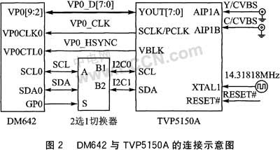 |
In Figure 2, the YOUR port of the TVP5150A is directly connected to the VP0 port of the DM642 for data transmission. The dot matrix clock line is connected to the VP0_CLK of the VP port on the DM642 for the clock signal for data transmission. The DM642 reads and writes the internal registers of the TVP5150A through the I2C bus to achieve the purpose of controlling the chip.
3.2 Video output section
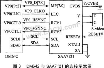
The VP0 A channel is used in the design for video playback. When playing back the collected data, the digital video signal needs to be reconverted into an analog signal before it can be played on the monitor. This conversion is done by the SAA7121 produced by Philips, and the circuit connection diagram of the video playback section is shown in Figure 3.
In Figure 3, the VP0 port of the DM642 outputs the digital video signal of the BT.656 format to the MP port of the SAA7121, and the Y signal and the Cb and Cr signals are separated by the internal data management module of the SAA7121 chip; and then sent to the corresponding analog/digital number in the chip. The conversion module converts the digital signal into an analog video signal; finally, it is output by CVBS (composite video signal) or Y, C (S-terminal signal) pins. The clock signal LLC of the SAA7121 is 27 MHz, which is provided by VP0CLK1 of the DM642, while the VP0CLK1 of the DM642 is derived from the SCLK pin of the TVP5150A, which enables synchronization of video acquisition and playback. The DM642 configures the 48 registers inside the SAA7121 chip through the I2C interface to control the chip.
 |
3.3 audio module
The audio codec chip in the system uses TI's TLV320AIC23B chip, which contains three interfaces: 1 serial control interface, connected to the I2C interface of the DM642; 2 analog audio interface for receiving analog audio from MITIN/LINEIN Signal, or analog audio signal output LINE-OUT; 3 digital audio interface for data transmission with the DM642's McASP port. The TLV320AIC23B receives the audio signal from the analog audio interface (MICIN/LINEIN), performs A/D conversion, and transmits the digital audio signal to the McASP of the DM642 through the digital interface for processing, and then saves it to the local hard disk along with the processed video signal. When playback is required, the digital audio data that has not been encoded is then transmitted back to the TLV320AIC23B by McASP, and after D/A conversion, it is output from the analog audio interface (LINEOUT). The DM642 configures and controls the chip through the I2C interface. The four TLV320AIC23B chips are connected to the I2C bus in the same way as the TVP5150A.
3.4 I2C bus
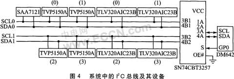
This system uses 4 video decoding chips, 4 audio codec chips and 1 video encoding chip. Each chip provides 2 slave addresses, so the system can complete 4 pairs by using only 2 sets of I2C bus. Control of the same type of chip. The DM642 chip itself only provides an I2C bus interface, so a 2-to-1 switch SN74CBT3257 is also required, so that the DM642 only receives one of the two I2C buses at a time. The connection diagram is shown in Figure 4.
 |
4 storage module
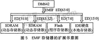
The DM642's EMIF address map in memory is divided into four independently addressable spaces CE[3:0], each occupying 256MB from address 0x80000000. These four addressing spaces can be configured according to the characteristics of the data width of the chip selected in the design. Among them, CE0 space is configured to 64-bit width, only for SDRAM memory mapping; CE1 space is configured for 8-bit width for Flash and UART mapping; CE2 space is configured for 16-bit width for ATA register mapping; CE3 Not used in this design, it can be used as a future expansion card. The extension diagram is shown in Figure 5.
 |
5 power module
The power module plays a pivotal role in the system design process. It consists of two parts: the power supply circuit and the power supply monitoring circuit.
5.1 Power supply circuit
The entire board is powered by +5 V and can be externally introduced or introduced from an extended PCI interface. The DM642 requires two independent voltages: the CPU core voltage GVDD (+1.4 V) and the peripheral I/O voltage DVDD (+3.3 V). These two voltages need to be strictly in order to supply power, that is, GVDD is earlier than DVDD, at least not later than DVDD. The design uses two TMS54310 power chips designed by TI for high performance DSP, FPGA, ASIC and microprocessor applications, providing CVDD and DVDD voltages to the DM642. Connect the PWRGD pin of the TPS54310(1) to the SS/EN pin of the TPS54310(2) on the circuit connection. When the output voltage of (1) is higher than 1.2 V, the chip (2) starts to work; when this value reaches a stable +1.4 V, the PWRGD pin outputs a high level to the SS/EN pin of the chip (2). . This ensures that the CPU core's power-on time is earlier than the I/O power-on time, as shown in Figure 6(a).
5.2 Power Monitoring Circuit
In order to ensure that the DM642 chip does not reach the required level when the power supply does not reach the required level, and allows each chip in the system to adjust the working state at any time by resetting, it is necessary to add a power supply monitoring system to the system. The circuit is shown in Figure 6(b). This circuit ensures that the DSP is always in a reset state until CVDD and DVDD reach the required level during system power-up. The TPS3823-33 chip produced by TI has been selected, and its fixed reset signal time is up to 200 ms, which can meet the reset requirements of all chips in the system. The chip has a watchdog circuit that receives timing signals from the CPU through the WDI pin to avoid system program runaway.
 |
Conclusion
The DM642's high-speed processing capability and excellent external interface capability make it superior to specialized video codecs in terms of image quality, hardware cost, flexibility and product updates. In terms of data storage, the system can not only select the local storage mode, but also use the EMAC interface provided in the DM642 to save the processed large amount of data to the server through the network, or save the data to the hard disk in the host through the PCI port. This ease of scalability gives users more choices in the actual use process.
references:
[1]. TVP5150A datasheet http://
[2]. SAA7121 datasheet http://
[3]. TLV320AIC23B datasheet http://
[4]. SN74CBT3257 datasheet http://
[5]. PCI datasheet http://
[6]. TPS54310 datasheet http://
[7]. TPS3823-33 datasheet http://
:
Rectangle Chafing Dish,Rectangle Chafing Dishes,Rectangle Chafing Dish With Spring Legs,Mobile Table Ware
Shaoxing Biaoyi Hardware Products Co., Ltd. , https://www.byeob.com